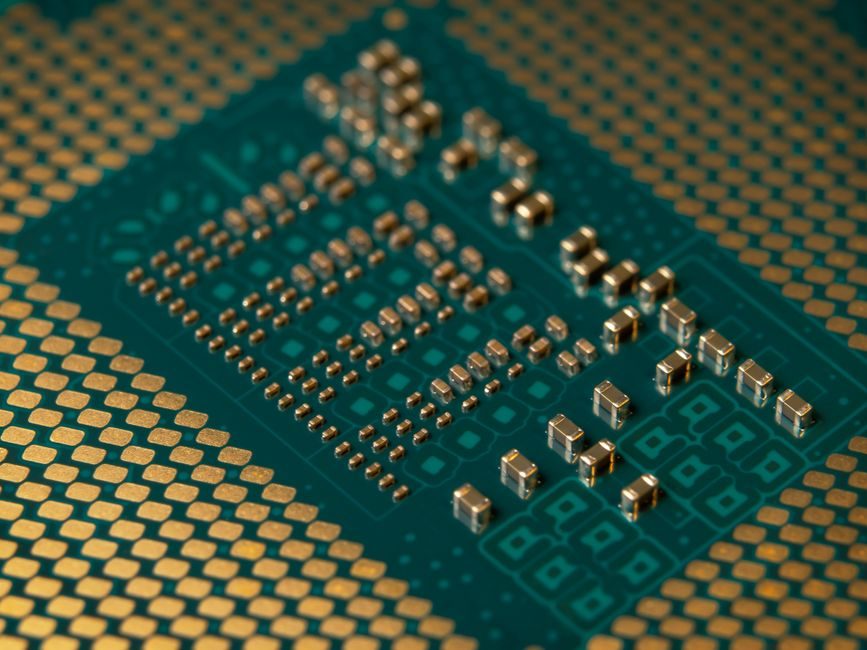
The reliability gate for any power semiconductor line is a 1000-3000 h burn-in screen where the FIT (failures in time) rate is the published figure, with stability of the reverse current under a stable reverse bias named as the single most informative parameter for catching infant-mortality parts [S3].
Two inspection layers bracket the process: AI-based machine vision from wafer alignment through PCB assembly to final packaging, and analytical techniques (large-area cross-section SEM, fault localisation) reserved for SiC and GaN compound-semiconductor failure analysis [S2][S5]. Vendor offerings in 2026 line up around CXP-12 and 5GigE area-scan cameras, line-scan TDI sensors, and SWIR/UV variants for sub-surface defect capture [S1].
Reliability parameters and the 1000-3000 h burn-in window
The Russian Electrical Engineering paper from 2019 formalises what most power-device QA teams already practice: the early-operation section of 1000-3000 h carries the dominant share of field failures, so screening is concentrated there rather than at the random-failure plateau [S3]. FIT rate is the parameter that scales to fleet-level reliability, and the paper argues reverse-current stability under a held reverse voltage is the single physical signal that predicts infant-mortality devices [S3].
That same paper cites OST 16-0.801.464-88 (a Soviet-era power-semiconductor reliability-testing standard) and a Mitsubishi 3rd-generation IGBT application manual as the working references for parameter selection [S3]. In a modern 2026 QA lab, the equivalent procedure is an automated test system that holds V_R, monitors I_R drift over the burn-in interval, and rejects parts whose I_R exceeds a defined threshold - a method published in Russ. Electr. Eng. 2016, vol. 87, no. 7 [S3].
Machine-vision inspection: interface, optics, and what each layer catches
CXP-12 and 5GigE area-scan cameras are the bandwidth backbone for high-throughput defect capture on patterned wafers, where sub-micron structures demand both pixel resolution and frame rate beyond what GigE delivers [S1]. Line-scan cameras with TDI (time-delay-integration) stages, such as the racer 2 TDI family, are specified for the continuous strip-and-stitch imaging of wafer edges, dicing streets, and back-grind surfaces where a single 2D frame would smear [S1].
Optics are not interchangeable: telecentric lenses with coaxial light coupling lock magnification across the field of view and remove perspective error - a hard requirement for die-height measurement and bond-pad planarity checks [S1]. SWIR and UV variants extend the spectral range; SWIR penetrates silicon to reveal sub-surface cracks and solder-void imaging, while UV highlights resist residues and organic contamination that visible-light systems miss [S1].
AI software layers now run on top of this hardware. Cognex's electronics portfolio uses AI-based golden-pose alignment to teach the system a known-good reference orientation, then flags any deviation - the relevant use cases are wafer alignment, PCB assembly, and final packaging [S2]. For power modules, that maps onto substrate-attach alignment, wire-bond or clip-bond position, and lid-seal inspection before the part leaves the line.
Failure analysis and characterisation on SiC / GaN devices
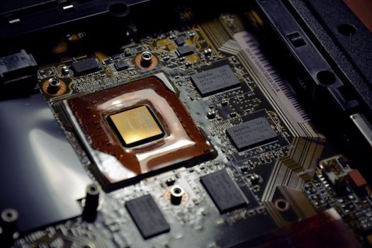
SiC and GaN power devices fail by mechanisms that do not always leave a visible signature at the surface - crystalline defects, mobile charge in the gate dielectric, and die-attach delamination are the recurring failure modes [S6]. Thermo Fisher's 2026 analytical portfolio addresses this with large-area cross-section SEM sample preparation, fault-localisation tooling, and electron-channeling contrast imaging to resolve dislocations in compound semiconductors [S5][S6].
For procurement, the practical signal is: when a power-module maker publishes a failure-analysis report citing SEM cross-section or ECCI imagery, it means the part has cleared a much higher bar than a datasheet curve trace. On-wafer parametric test plus post-fab SEM/FIB review is the chain that catches die-attach voids under the source pad, which are invisible to optical AOI but kill thermal-cycling life [S5].
Comparing the three QA pillars side by side
The three pillars of power-semiconductor QA - electrical burn-in, optical/AI machine vision, and SEM/FIB failure analysis - are not redundant. Burn-in catches parametric drift on every shipped unit, machine vision catches geometric and surface defects on 100% of parts at line speed, and SEM/FIB is destructive and applied to a sampled subset for root-cause work [S3][S1][S5].
On throughput, machine vision leads: CXP-12 frame grabbers and 5GigE interfaces move multi-megapixel images at line cycle times measured in milliseconds per die [S1]. On defect sensitivity, SEM/FIB leads: it resolves features below 100 nm and identifies crystalline defects invisible to optical methods [S5]. On cost per part, burn-in dominates the bill because the 1000-3000 h interval ties up test sockets and bias supplies, but it is also the only method that publishes a fleet-level FIT number [S3].
Procurement-side signals to track in 2026

Three signals are worth watching on supplier datasheets and qualification reports. First, FIT rate - a supplier quoting sub-10 FIT at 1000 h with a stated confidence interval is running a real burn-in screen; a missing or "typical" label is a red flag [S3]. Second, the camera interface and lens stack on the inspection line - a CXP-12 plus telecentric-lens spec tells you the supplier is resolving features that a USB 3.0 system with a fixed-focal lens will miss [S1]. Third, whether the supplier publishes a failure-analysis methodology for SiC/GaN parts - SEM cross-section plus ECCI is the current state of the art, and its absence means the supplier is treating compound semiconductors as if they were silicon [S5][S6].
Adjacent reference material on this site covers power meter selection and spec mapping, MEMS sensor test and packaging cost breakdowns, and aluminum alloy choices for energy equipment - all useful when qualifying a power-module line that mixes semiconductor die, leadframe, baseplate, and housing materials. For readers mapping the wider electronics QA chain, our power meter and insulation tester spec guide and the MEMS capacity-planning piece cover adjacent burn-in and yield trade-offs.
Closing: in 2026, expect the FIT-rate disclosure to migrate from proprietary datasheet appendices into public qualification reports, and expect AI-vision defect libraries for SiC/GaN-specific failure modes to ship as vendor reference datasets rather than customer-built models. The next spec to watch is ECCI-based crystalline-defect quantification becoming a standard line item in SiC MOSFET failure-analysis reports [S6].
For the relevant spec sheets and selection criteria, see power quality analyzer, additive manufacturing material, and air quality monitor.