Power-device fabs running 200 mm Si, 150 mm SiC and 200 mm GaN-on-Si lines are absorbing the same Industry-4.0 retrofit wave that hit logic fabs five years earlier, with 2026 vendor offerings centred on AI-vision inspection, automated material-handling and process-control loops tuned for wide-bandgap (WBG) thermal budgets [S1][S3].
Vendors such as Sancode now market integrated OSAT, supply-chain and R&D automation bundles aimed at discrete-device packagers, while Murata's power-semi division serves the module-level side; Semiconductor Engineering's 2026 deep-dive covers WBG reliability, thermal characterisation and board-level packaging work that the automation stack must protect [S1][S2][S3].
Scope: What "Smart Manufacturing" Means for a Power-Device Line in 2026
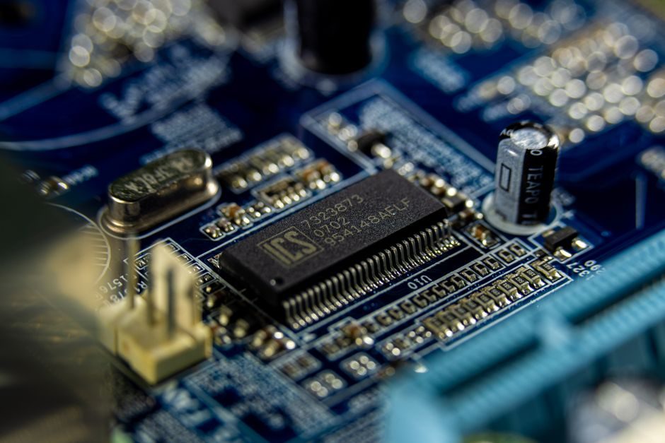
Smart manufacturing on a power-semiconductor line is the layering of MES, AMHS, in-line metrology and AI-driven process control on top of the wafer-to-die flow, with the wafer stage covering Si IGBT/MOSFET front-end, the SiC and GaN front-end, and the back-end covering thin-wafer dicing, die attach (sintered Ag, solder) and wire/clip bond — the automation stack has to straddle all of them, not just the front-end [S1][S3].
Discrete and module packaging are higher-mix, lower-volume than CMOS logic, which is why the 2026 retrofit conversation is dominated by OSAT-style vendors offering turnkey AI + IoT bundles rather than tool-by-tool upgrades — the goal is throughput at acceptable yield for SKUs that change every 1–2 quarters [S1].
Selection Criteria: Sensors, Connectivity and the Protocol Stack That Holds It Together
Equipment-side sensing leans heavily on industrial camera systems for solder-paste, die-placement and lead-frame vision, and on thermal/process instrumentation tied into smart meters and valve-positioner loops wherever wet benches or vacuum handlers feed into the tool — picking cameras and field instruments purely on price breaks the closed-loop control story that justifies the retrofit [S1].
Connectivity on the shop floor is still dominated by Ethernet, EtherCAT and OPC UA, with IO-Link for sensor-to-gateway edge wiring and MQTT for upstream MES/ERP hand-off; AI sits on top as a process-control layer, not a replacement for the field network [S1].
Power-quality and load-side metering on the tool chiller, vacuum pump and epitaxial-reactor RF generators is increasingly pulled from power meters and from the same power cable infrastructure that feeds the fab substation — energy-per-wafer and energy-per-die are now standard MES tags, and they are the easiest retrofit win on a power-device line.
Who This Stack Is FOR, and Who Should NOT Buy It

The 2026 OSAT-style retrofit fits discrete IGBT/MOSFET packagers running 5,000–50,000 wafer-equivalents/month, SiC-module houses on 150 mm moving to 200 mm, and GaN-on-Si lines that need automated handling of thinner, more brittle wafers [S1][S3]. It also fits mixed-signal/analog fabs adding a power-semi line as a second product stream, where the existing AMHS, MES and quality systems can absorb the new tool set with limited re-validation [S1].
It is a poor fit for captive IDM lines already running fully integrated Industry-4.0 stacks (Infineon, onsemi, ST, Wolfspeed-class sites), for very low-volume R&D fabs below ~500 wafers/month, and for any project where the upstream WBG epitaxy or back-grinding process is still unstable — automation amplifies an unstable process rather than fixing it, so MES + AI retrofits should follow process stabilisation, not precede it [S1][S3].
Option Comparison: Three 2026 Automation Approaches Side by Side
Process engineers typically pick from three delivery models, and the right one depends on in-house MES/AMHS maturity, not on brand loyalty. [S1]
Turnkey OSAT retrofit (Sancode-style): vendor delivers AI-vision stations, AMHS, MES templates and supply-chain integration as one contract; best for greenfield discrete packagers and brownfield lines with no MES; capex-heavy, fastest time-to-yield, lowest integration risk on the shop-floor software side [S1].
Tool-vendor automation (e.g. back-end equipment makers bundling vision, traceability and APC hooks): best for lines that already have a strong MES and want to standardise on one tool family; lowest per-tool integration cost but vendor lock-in is real, and the AI layer is usually a thin process-control module on top of the tool's own software [S1].
DIY / system-integrator model: customer owns the stack, system integrator (Siemens, Rockwell, Honeywell, local SIs) assembles cameras, IO-Link, OPC UA, MES and analytics; lowest licence cost, highest internal headcount cost, and the path that captive IDMs almost always take — recommended only where the fab already runs 24/7 internal automation engineering [S1].
WBG-Specific Automation Requirements: SiC and GaN Add Hard Constraints
SiC lines run hotter — epitaxy at 1,500–1,700 °C, high-temperature implant activation, and aggressive back-grinding to 100–175 µm final thickness — which forces thermal-aware process control and stricter AMHS wafer handling, and is a driver for inline thermal-characterisation work covered in the 2026 Semiconductor Engineering deep-dive [S3].
GaN-on-Si is the other end of the constraint set: 200 mm Si substrates, thinner epitaxy, no high-temp activation step, but extreme sensitivity to wafer bow and to electrostatic discharge, which pushes for grounded FOUPs, ioniser-monitored smart camera stations and AI-driven in-line metrology that flags sub-pixel anomalies before dicing [S1][S3].
Reliability programmes for both WBG families are now built into the automation stack, not bolted on: high-temperature gate-bias (HTGB), H3TRB and power-cycling data flow into the same MES that tracks inline electrical test, and lifetime-prediction models feed back into process windows — this is the "closed-loop" story the 2026 OSAT vendors are selling [S3].
Use Cases: Where 2026 Retrofits Are Landing First
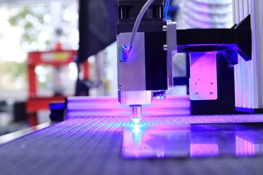
Discrete IGBT packagers are deploying AI-vision for lead-frame solder joint inspection, automated optical inspection of sintered Ag die-attach, and inline X-ray for voiding control — these are the high-yield, fast-payback retrofits that an OSAT bundle can stand up in a single quarter [S1].
SiC-module houses are the second wave: 200 mm SiC line builders are integrating AMHS, cleanroom robotics and AI-driven CMP polish-endpoint control from day one, partly because the silicon wafer smart manufacturing playbook already exists and is being copied almost line-for-line, and partly because SiC wafer cost makes any yield loss painful [S3].
GaN-on-Si power lines are the third wave, and the hardest: automation vendors have to combine ESD-safe handling, in-line bow/warp metrology and fast recipe switching for short GaN product cycles — the closest parallel is the EV inverter GaN ramp, where power semiconductor manufacturing process lines built in 2025–2026 are the reference designs that later projects are cloned from [S3].
Limitations, Failure Modes and Sourcing Risk

The biggest 2026 failure mode is process instability masked by automation: AI-vision catches defects that the upstream process created, and the line throws good die after good die because the root cause is never closed — engineers should treat the AI layer as a sensor, not a solution, and gate MES/AI retrofits behind a process-capability review [S1].
Supply-chain risk is the second limitation: high-end industrial cameras, vision processors and 6-axis cleanroom robots are still constrained in 2026, and any industrial robot supply shortage 2026 ripple is amplified on a power-semi line because cleanroom-rated units are a small fraction of the total market [S1].
Standards coverage is uneven: OPC UA companion specs for power-semi-specific processes (sinter profile, clip bond, H3TRB) are still maturing, and a fab that bets on a single vendor's proprietary data model will pay later when MES migration comes around — preference for open, IEC-compliant interfaces is the safer 2026 default [S1][S3].
A practical 2026 sourcing map also needs to account for raw materials: GaN-on-Si pulls from the same silicon and rare-earth process consumables covered in the copper smart manufacturing and top rare earth companies 2026 flows, and SiC powder/wafer supply is the single biggest choke point for any SiC retrofit timeline [S3].
For context on the back-end side, a harmonic drive reducer 2026 price and cost guide shows why cleanroom robot pricing is sticky: precision reducers and cleanroom-rated motors are not commoditised, and that pricing floor is what makes a 2026 OSAT retrofit capex number what it is.